Author Affiliations
Abstract
1 School of Nano Technology and Nano Bionics, University of Science and Technology of China, Hefei 230026, China
2 Nano Fabrication Facility, Suzhou Institute of Nano-Tech and Nano-Bionics, Chinese Academy of Sciences, Suzhou 215123, China
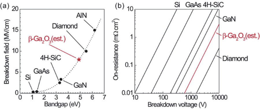
Power electronic devices are of great importance in modern society. After decades of development, Si power devices have approached their material limits with only incremental improvements and large conversion losses. As the demand for electronic components with high efficiency dramatically increasing, new materials are needed for power device fabrication. Beta-phase gallium oxide, an ultra-wide bandgap semiconductor, has been considered as a promising candidate, and various β-Ga2O3 power devices with high breakdown voltages have been demonstrated. However, the realization of enhancement-mode (E-mode) β-Ga2O3 field-effect transistors (FETs) is still challenging, which is a critical problem for a myriad of power electronic applications. Recently, researchers have made some progress on E-mode β-Ga2O3 FETs via various methods, and several novel structures have been fabricated. This article gives a review of the material growth, devices and properties of these E-mode β-Ga2O3 FETs. The key challenges and future directions in E-mode β-Ga2O3 FETs are also discussed.
enhancement mode FETs β-Ga2O3 Journal of Semiconductors
2023, 44(6): 061801
1 桂林电子科技大学 广西精密导航技术与应用重点实验室, 广西 桂林 541004
2 中国科学院苏州纳米技术与纳米仿生研究所 纳米加工平台, 江苏 苏州 215123
3 中国科学技术大学 纳米技术与纳米仿生学院, 合肥 215123
4 南京理工大学 材料科学与工程学院, 南京 210000
提出了一种并联体声波谐振器(BAWR)与Ga2O3基MSM紫外传感器的新型高灵敏度传感器结构, 即体声波谐振式日盲紫外光传感器(BAWR-UV Sensor)。设计并制备了MSM Ga2O3紫外传感器和BAWR传感器, 将实测的光、暗S参数在仿真软件中封装为S1P数据模型代替MSM等效电路, 用MBVD模型代替BAWR等效电路, 通过并联两种结构建立了BAWR-UV仿真模型; 采用ADS软件仿真了BAWR核心参数对BAWR-UV传感器灵敏度的影响, 研究了提高灵敏度的设计方案。仿真结果表明, 在0.5~4.5GHz频率范围内, BAWR-UV的并联Q值越大, 阻抗灵敏度越高, 同时阻抗灵敏度随频率降低而增大, 在并联谐振频率fp=0.533GHz时获得最佳阻抗灵敏度为100kΩ/(μW/mm2); 频率灵敏度随频率的升高而增大, 在fp=4.5GHz时获得最佳频率灵敏度为1.4MHz/(μW/mm2)。最后, 开展了高灵敏度日盲紫外传感器的探索。
日盲紫外探测器 体声波谐振器 氧化镓 叉指传感器 solar blind ultraviolet detector bulk acoustic wave resonator gallium oxide interdigital sensor

Author Affiliations
Abstract
1 State Key Laboratory on High Power Semiconductor Lasers, Changchun University of Science and Technology, Changchun 130022, China
2 Nanofabrication Facility, Suzhou Institute of Nano-Tech and Nano-Bionics, Chinese Academy of Sciences, Suzhou 215123, China
GaN has been widely used in the fabrication of ultraviolet photodetectors because of its outstanding properties. In this paper, we report a graphene–GaN nanorod heterostructure photodetector with fast photoresponse in the UV range. GaN nanorods were fabricated by a combination mode of dry etching and wet etching. Furthermore, a graphene–GaN nanorod heterostructure ultraviolet detector was fabricated and its photoelectric properties were measured. The device exhibits a fast photoresponse in the UV range. The rising time and falling time of the transient response were 13 and 8 ms, respectively. A high photovoltaic responsivity up to 13.9 A/W and external quantum efficiency up to 479% were realized at the UV range. The specific detectivity D* = 1.44 × 10¹⁰ Jones was obtained at –1 V bias in ambient conditions. The spectral response was measured and the highest response was observed at the 360 nm band.
Journal of Semiconductors
2022, 43(6): 062804
Author Affiliations
Abstract
1 School of Science, Changchun University of Science and Technology, Changchun 130022, China
2 Suzhou Institute of Nano-Tech and Nano-Bionics, Chinese Academy of Sciences, Suzhou 215123, China
3 School of Materials Science and Engineering, Nanjing University of Science and Technology, Nanjing 210094, China
A monolithic integrated ultraviolet-infrared (UV-IR) dual-color photodetector based on graphene/GaN heterojunction was fabricated by vertically integrating a GaN nanowire array on a silicon substrate with monolayer graphene. The device detects UV and IR lights by different mechanisms. The UV detection is accomplished by the forbidden band absorption of GaN, and the IR detection is realized by the free electron absorption of graphene. At peak wavelengths of 360 nm and 1540 nm, the detector has responsivities up to 6.93 A/W and 0.11 A/W, detection efficiencies of 1.23 × 1012 cm·Hz1/2 ·W-1 and 1.88 × 1010 cm·Hz1/2 ·W-1, respectively, and a short response time of less than 3 ms.
UV-IR dual-color photodetector heterojunction GaN nanowire array graphene Chinese Optics Letters
2020, 18(11): 112501


